Summary
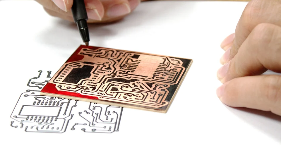
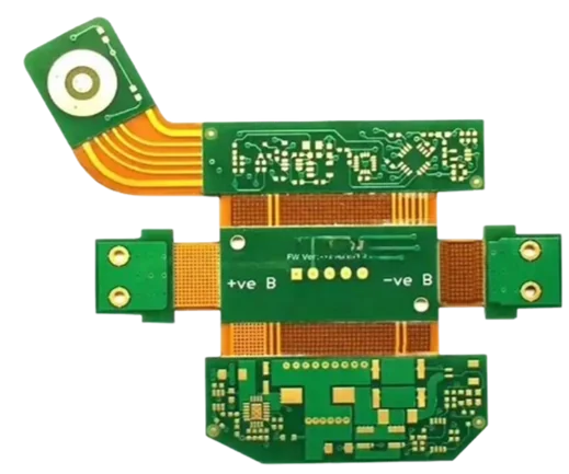
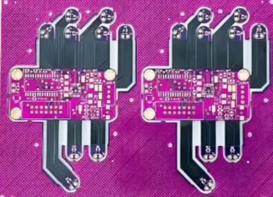
Senior PCB Design Engineers with 15 years of experience specialize in FR4, metal-clad, rigid-flex, and flex PCBs, handling complex multi-layer, high-speed, analog, digital, RF, high-power, and power circuits. They lead PCB layout and DFMA reviews, generate schematics/footprints, create Gerber files, panel validation, stencil/DXF/STEP/XY reports, and manufacturing data while ensuring DFM/DFA/DFT, IPC standards (782A, 7351A, 2221/2222), EMI/RFI/ESD mitigation, and thermal management.
Key Capabilities
- Design and route high-speed/RF signals with impedance control, differential pairs, stack-up optimization, and signal/power integrity.
- Manage ECAD libraries, templates, Gerber releases, and CAD licensing; interface with hardware/mechanical teams and vendors for fabrication/assembly.
- Conduct production support, VAVE improvements, and cross-functional reviews to reduce costs, EMI, and time-to-market.
- Knowledge of modern SMT packaging with a thorough understanding of the PCB fabrication process and IPC standards.
Primary Responsibilities
- Lead schematic generation, footprint creation, PCB layout/routing, Gerber/assembly file generation, and validation checks.
- Perform layout studies for manufacturability, create/update best practices checklists/workflows, and provide training/mentorship to juniors.
- Collaborate on design reviews, resolve vendor issues, and document processes from concept to mass production.
Secondary Responsibilities
- Maintain/upgrade existing designs, handle engineering changes, and monitor production processes.
- Offer technical consultation to project managers and participate in continuous improvement teams for quality/cost reduction.
- Comfortable dealing with suppliers for PCB/FPC fabrication and assembly.
- Participate on cross-functional teams to ensure the continuous, on-going improvement of processes, methods, productivity and quality, while reducing costs.
PCB Layout
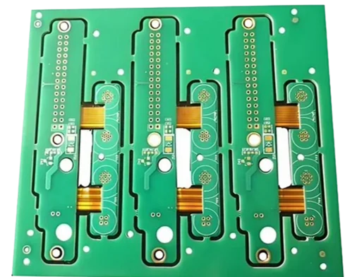
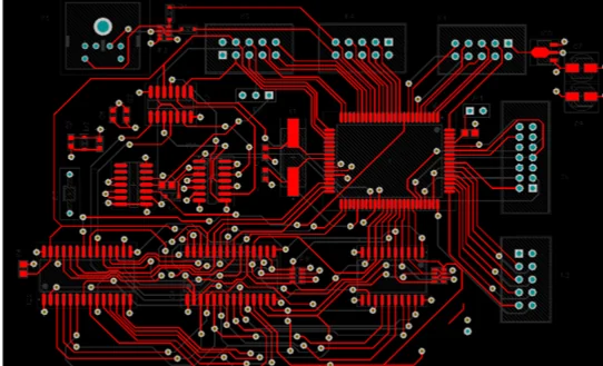
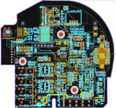
Multi-layer, RF, high-speed, rigid-flex, flex, power, and fabrication-ready PCB routing and stack-up design.
Manufacturing
Gerber generation, stencil/DXF/STEP/XY outputs, DFMA reviews, panel validation, and vendor coordination.
Compliance
IPC standards, EMI/RFI/ESD mitigation, thermal management, DFM/DFA/DFT, and production support workflows.
Need PCB design support?
Reach out for schematic capture, PCB layout, DFMA reviews, Gerber generation, manufacturing data preparation, and high-performance board design support.